Get Involved
Society of Physics Students

The Society of Physics Students (SPS) is a professional association explicitly designed for students and their advisers. Membership, through collegiate chapters, is open to anyone interested in physics. The only requirement for membership is that you be interested in physics. Besides physics majors, our members include majors in astronomy, chemistry, computer science, engineering, geology, mathematics, medicine, and other fields. SPS is open to everyone.
Sigma Pi Sigma
Sigma Pi Sigma exists to honor outstanding scholarship in physics and astronomy; to encourage interest in physics and astronomy among students at all levels; to promote an attitude of service of its members towards their fellow students, colleagues, and the public; to provide a fellowship of persons who have excelled in physics and astronomy.
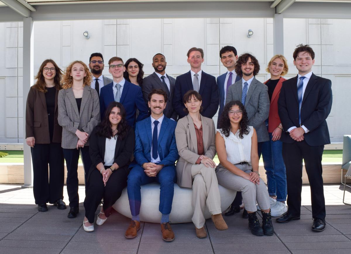
Chapters in Action


Find a Chapter
Alumni

SPS and Sigma Pi Sigma want to ensure that alumni stay involved and help current undergraduates in the physical sciences! Whether this is being open to attending events held by SPS and/or Sigma Pi Sigma chapters, participating in workshops geared towards professional development and helping us understand what undergraduates need, speaking on our podcast about your career journey, and more! We have programs to meet every alum at your availability.
Physics & Astronomy Congress

The Physics and Astronomy Congress is the largest gathering of undergraduate physics and astronomy students in the world. Every three years, it brings together physics students, alumni, and faculty members for three days of frontier physics, workshops, networking, and fun. The event is supported by the American Institute of Physics and hosted by Sigma Pi Sigma, the physics and astronomy honor society. Anyone interested in physics and astronomy is invited to attend!
Member Achievements
Apply for an Award


Upcoming Events
Submit an Event